
Turn abandoned patents
into your own filing
into your own filing
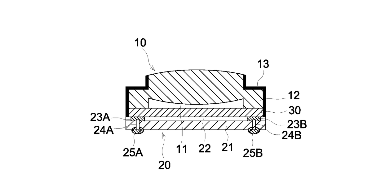
This invention describes a method for manufacturing compact camera modules, such as those found in smartphones. It integrates light control directly into the lens structure by forming a light-blocking layer on the sides of the lenses and their support components. This layer acts as both a diaphragm to regulate incoming light and a shield against stray light, eliminating the need for separate parts and simplifying the module. The method involves preparing image sensor wafers and lens arrays.
Why it matters: Wafer-level optics manufacturing has matured significantly since 2008, making the precise, integrated light shielding described here more feasible and cost-effective for mass production of compact camera modules.
AI gives you a few directions you could take this. Pick one, and we check whether your version is different enough to patent, then write the filing.
Reinvent this with AI


