
Turn abandoned patents
into your own filing
into your own filing
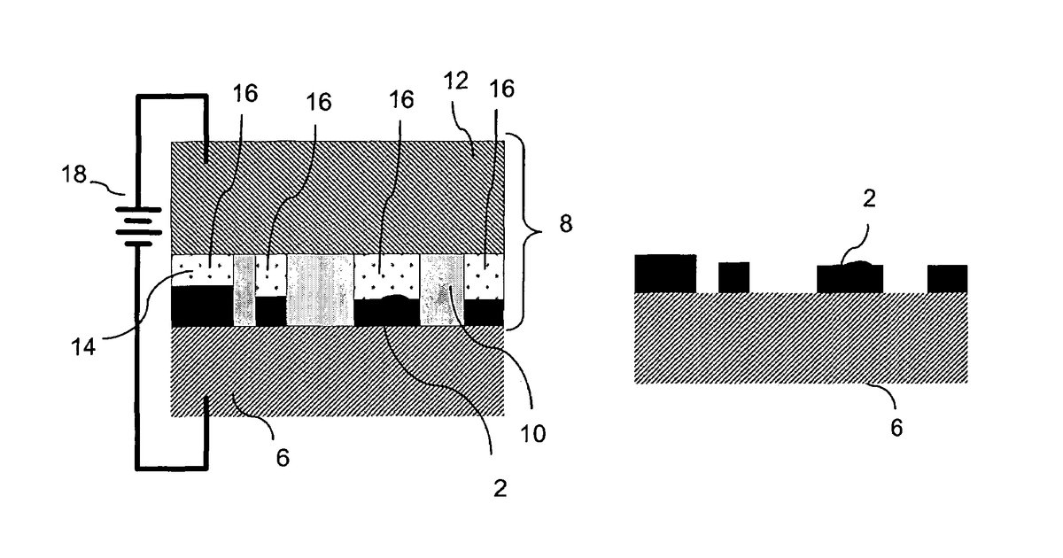
This describes a method for building tiny, intricate 3D objects by stacking many thin layers. It uses electroplating to deposit material, often incorporating insulating sheets, and then shapes each layer using masks. The masks can be transferred onto the surface or printed directly, for example, with an inkjet. The process specifically requires that at least one of the materials used in the structure is an insulating (dielectric) material.
Why it matters: Filed before the widespread advancement of high-resolution, multi-material additive manufacturing and micro-dispensing technologies. The precision and material versatility of computer-controlled inkjet and extrusion for mask patterning at the microscale have significantly improved since 2005.
AI gives you a few directions you could take this. Pick one, and we check whether your version is different enough to patent, then write the filing.
Reinvent this with AI


