
Turn abandoned patents
into your own filing
into your own filing
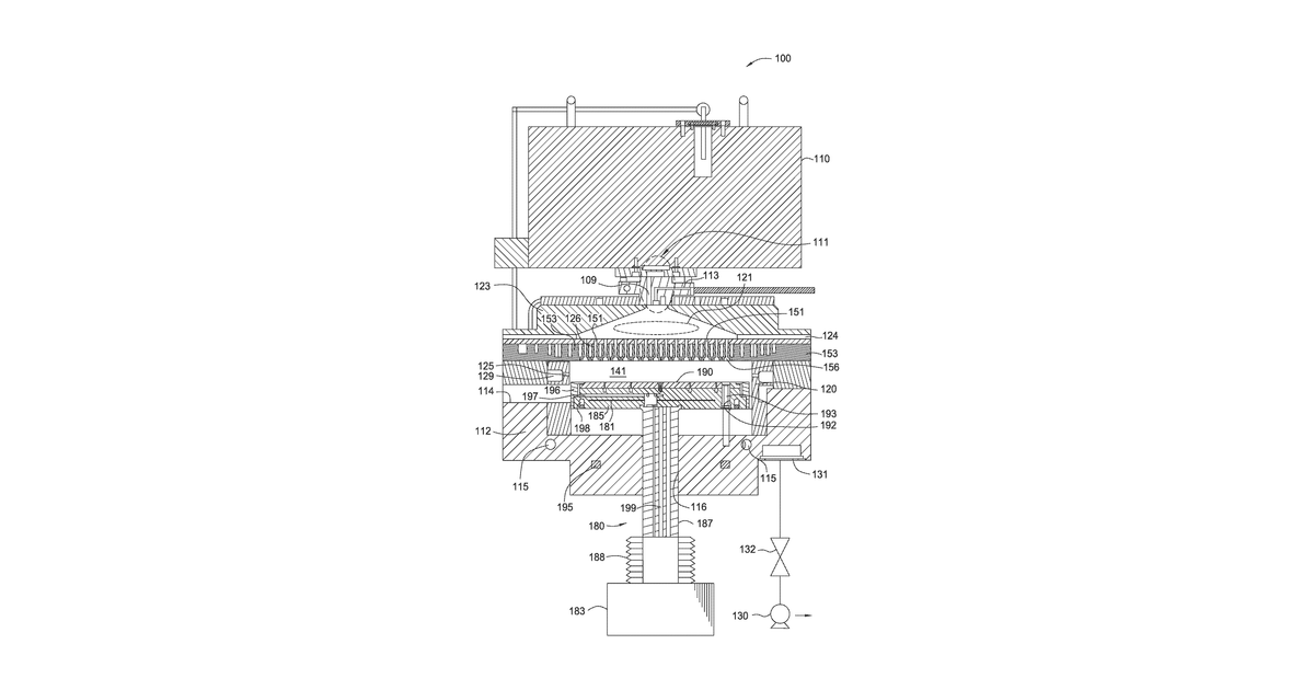
This invention describes a method for creating tiny components for semiconductor devices. It involves forming an extremely thin layer of a specific material, such as MoS2 or WS2, on a base, then heating that layer, and finally adding a protective top layer. All these steps are performed sequentially within a specialized processing system without ever exposing the material to air.
Why it matters: Continued advancements in atomic layer deposition and chemical vapor deposition for 2D materials, alongside improved in-situ process control within vacuum cluster systems, may now offer better prospects for achieving the required material quality and uniformity for semiconductor integration.
AI gives you a few directions you could take this. Pick one, and we check whether your version is different enough to patent, then write the filing.
Reinvent this with AI


