
Turn abandoned patents
into your own filing
into your own filing
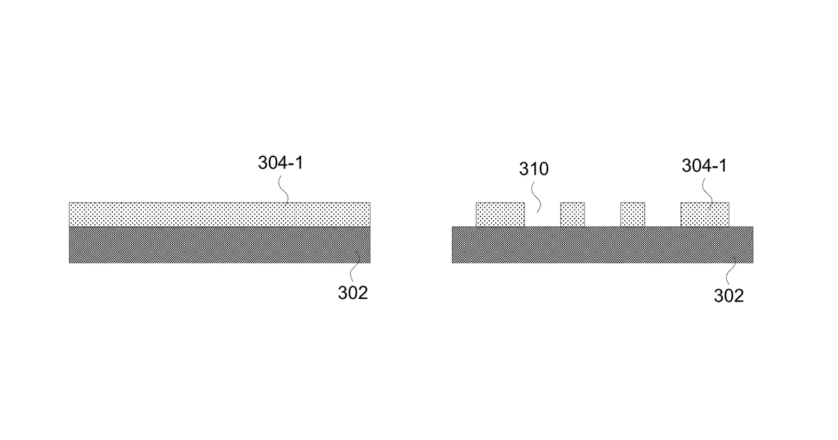
This invention describes a method for building tiny 3D metal objects, like components for devices, by stacking up many thin layers. Each layer is formed by precisely depositing both conductive metal and insulating material. A key feature is that the insulating material can be selectively placed without needing a physical stencil or mask.
Why it matters: Filed before the widespread maturation of multi-material micro-3D printing. The maskless selective deposition of dielectrics is now more achievable with advanced additive manufacturing systems.
AI gives you a few directions you could take this. Pick one, and we check whether your version is different enough to patent, then write the filing.
Reinvent this with AI


