
Turn abandoned patents
into your own filing
into your own filing
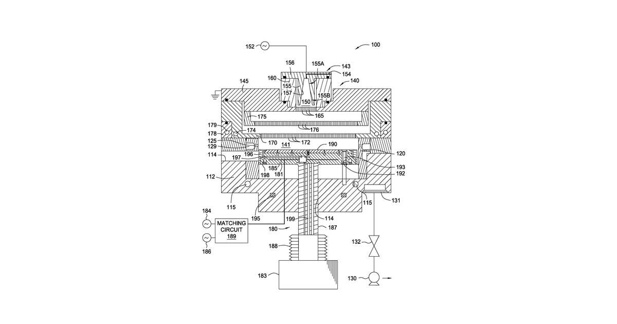
This invention describes a way to remove a protective layer from a silicon wafer using a special etching process. It involves treating the layer, then using a remotely generated plasma from a specific gas mixture (ammonium and nitrogen trifluoride) to etch it away at a low temperature. After etching, the layer is plasma annealed and a new protective layer is added to stabilize the surface.
Why it matters: The increasing complexity and miniaturization of semiconductor devices since 2013 have made precise interface control and minimized queue time degradation more critical for yield.
AI gives you a few directions you could take this. Pick one, and we check whether your version is different enough to patent, then write the filing.
Reinvent this with AI


