
Turn abandoned patents
into your own filing
into your own filing
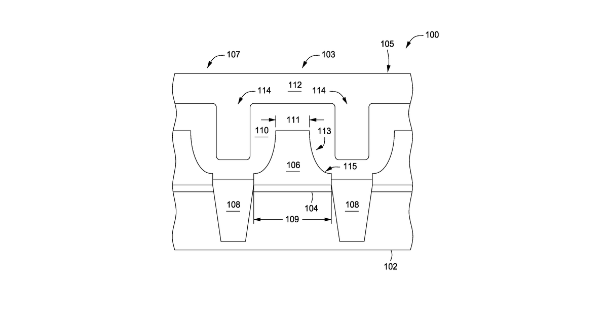
This invention describes a machine that shapes tiny layers of material, such as those used in computer chips, by repeatedly forming and then removing a thin oxide layer from its surface. The machine performs these steps in a single chamber, etching the material at a low temperature (below 100°C) and then oxidizing it at a much higher temperature (between 200°C and 1000°C) to achieve the desired shape.
Why it matters: Filed in 2010, this technology predates the widespread maturity of Atomic Layer Etching (ALE) and advanced Atomic Layer Deposition (ALD) for precise material shaping. The continued drive for extremely narrow pitch semiconductor devices, especially for memory, makes such cyclical, atomic-scale processing more critical and feasible today.
AI gives you a few directions you could take this. Pick one, and we check whether your version is different enough to patent, then write the filing.
Reinvent this with AI


