
Turn abandoned patents
into your own filing
into your own filing
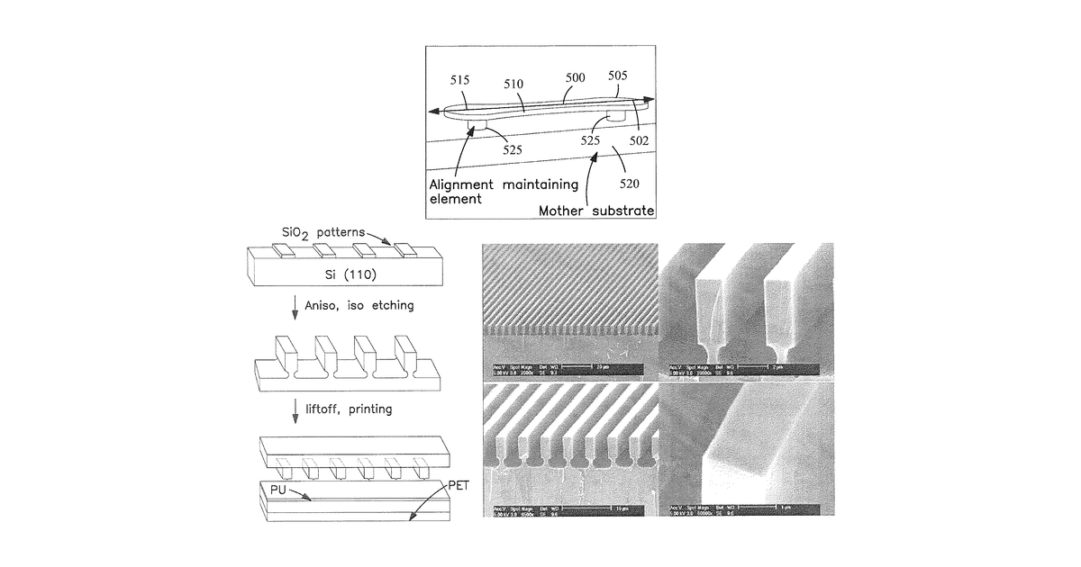
This invention describes a way to make electronic devices by placing tiny, solid semiconductor pieces onto a surface. These semiconductor pieces are designed to be printed and are held in precise position by small, broken-off alignment parts. The claims specifically focus on devices where these semiconductor pieces are single, inorganic structures, often held by two such fractured alignment elements.
Why it matters: Filed in 2021, this invention relies on advanced nanoscale fabrication and assembly. Since then, ongoing progress in high-resolution additive manufacturing and micro-assembly techniques may have improved the precision and efficiency required for creating such printable semiconductor devices.
AI gives you a few directions you could take this. Pick one, and we check whether your version is different enough to patent, then write the filing.
Reinvent this with AI


