
Turn abandoned patents
into your own filing
into your own filing
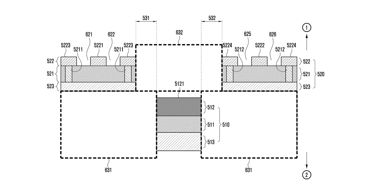
This invention describes a flexible circuit board designed for transmitting high-frequency signals within an electronic device. It achieves this by separating power lines from signal lines into different stacked layers. Crucially, specific cut-outs, or slits, are made in these layers where they overlap, creating a through-hole in the board to improve signal performance and reduce interference.
Why it matters: The continued miniaturization and higher frequency demands in devices like foldable phones and AR/VR headsets have intensified the need for advanced flexible PCB designs that manage signal integrity and power delivery. Manufacturing techniques for such complex flexible PCBs may have advanced, making this design more feasible.
AI gives you a few directions you could take this. Pick one, and we check whether your version is different enough to patent, then write the filing.
Reinvent this with AI


