
Turn abandoned patents
into your own filing
into your own filing
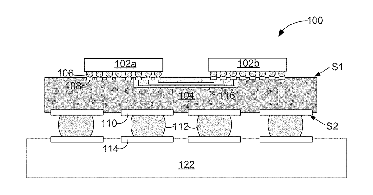
This invention describes a manufacturing process for a specialized base, called a package substrate, used to connect computer chips. The process ensures that one side of the substrate, where lands are located, receives a specific outermost finish, while the opposite side, where chip connection pads are, receives a different outermost finish. This is achieved by carefully applying and removing protective layers during the finishing steps.
Why it matters: The period since 2019 has seen rapid advancements in advanced packaging for AI and high-performance computing. This method for precise dual-sided surface finishing could now be more critical for optimizing complex chip interconnects and thermal performance in these demanding applications.
AI gives you a few directions you could take this. Pick one, and we check whether your version is different enough to patent, then write the filing.
Reinvent this with AI


