
Turn abandoned patents
into your own filing
into your own filing
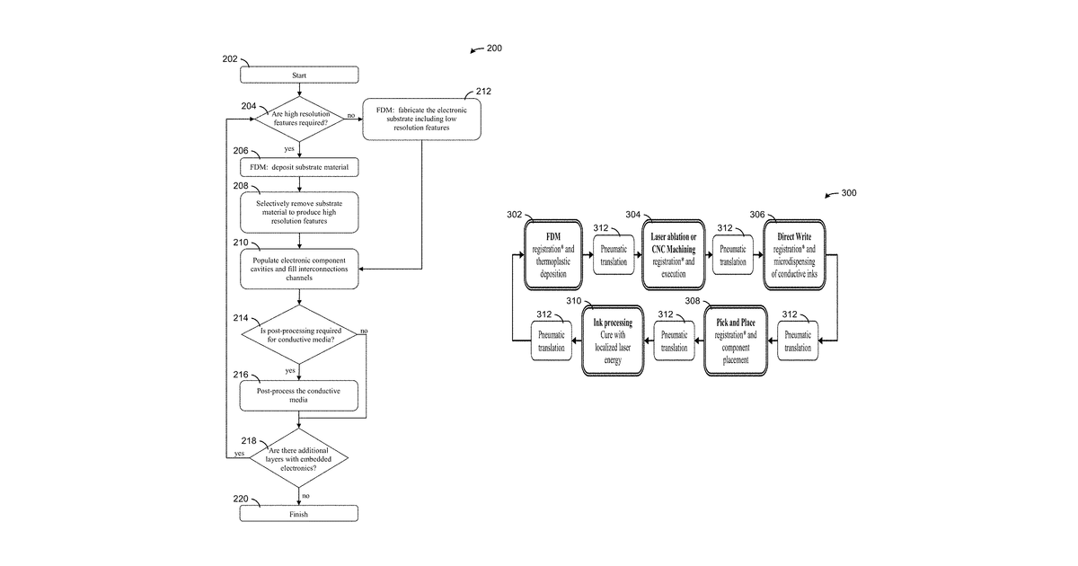
This invention describes a way to make three-dimensional electronic devices by building up a plastic structure layer-by-layer using a 3D printer that melts and deposits plastic, known as Fused Deposition Modeling (FDM). This plastic structure is designed with tiny holes and spaces. Once the structure is printed, conductive material is used to fill the holes, creating electrical connections, and electronic components are placed into the designated spaces.
Why it matters: Filed before multi-material FDM and integrated component placement were common. These technologies are now more accessible and precise, simplifying system integration.
AI gives you a few directions you could take this. Pick one, and we check whether your version is different enough to patent, then write the filing.
Reinvent this with AI


