
Turn abandoned patents
into your own filing
into your own filing
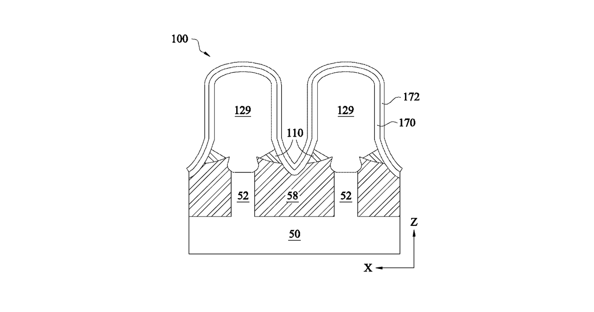
This invention describes a detailed recipe for building tiny, efficient computer switches called FinFETs. It involves carving out thin walls, or "fins," on a silicon chip, then carefully growing additional material on these fins, and precisely shaping the surrounding insulating layers. The patent specifically covers the step-by-step process for creating these advanced transistor structures.
Why it matters: FinFET technology has matured significantly since 2015, and advancements in precision epitaxial growth and etching techniques now allow for more intricate and controlled fin structures. This could make the specific manufacturing steps for creating pillar-shaped epitaxial fins more feasible or efficient than when the patent was filed.
AI gives you a few directions you could take this. Pick one, and we check whether your version is different enough to patent, then write the filing.
Reinvent this with AI


