
Turn abandoned patents
into your own filing
into your own filing
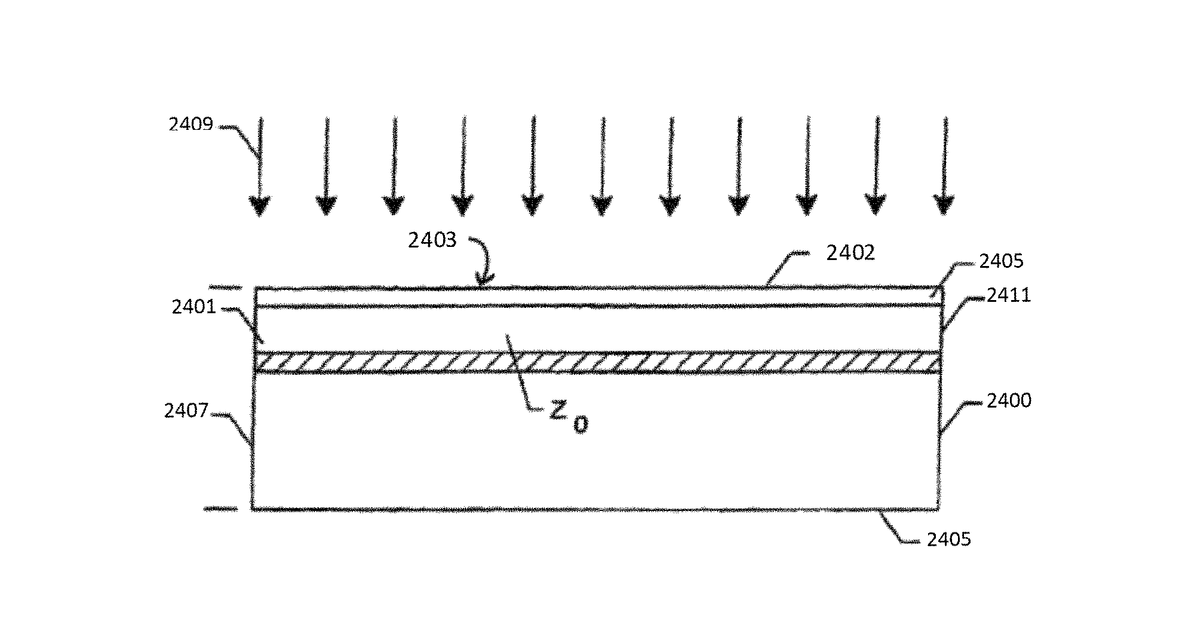
This invention describes a way to make very thin layers of Gallium Nitride (GaN) material. It involves taking a piece of GaN, adding a layer of silicon dioxide and then aluminum nitride to its surface, and then bonding that surface to an insulating base material. Next, tiny particles are shot into the GaN to create a weak spot, allowing a very thin film of GaN to be precisely broken off and left attached to the insulating base.
Why it matters: The method creates thin GaN layers on insulating substrates. Since 2014, the rapid growth of GaN power and RF device markets has increased the need for advanced GaN-on-insulator manufacturing, and improvements in precise ion implantation and multi-layer wafer bonding may now enable this specific process more effectively.
AI gives you a few directions you could take this. Pick one, and we check whether your version is different enough to patent, then write the filing.
Reinvent this with AI


